Socket 370
 | |
| Release date | 1998 |
|---|---|
| Designed by | Intel |
| Type | PGA-ZIF |
| Chip form factors | Plastic pin grid array (PPGA) and Flip-chip pin grid array (FC-PGA and FC-PGA2) |
| Contacts | 370[1] |
| FSB protocol | AGTL+, AGTL |
| FSB frequency | 66, 100 and 133 MT/s |
| Voltage range | 1.05–2.1 V |
| Processor dimensions | 1.95 × 1.95 inches[2] (49.53 mm x 49.53 mm) |
| Processors | Intel Celeron Mendocino (PPGA, 300–533 MHz, 2.0 V) Intel Celeron Coppermine (FC-PGA, 533–1100 MHz, 1.5–1.75 V) |
| Predecessor | Slot 1 |
| Successor | Socket 423 |
This article is part of the CPU socket series | |
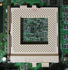
Socket 370, also known as PGA370, is a CPU socket first used by Intel for Pentium III and Celeron processors to first complement and later replace the older Slot 1 CPU interface on personal computers. The "370" refers to the number of pin holes in the socket for CPU pins.
Socket 370 was replaced by Socket 423 in 2000.
Overview

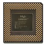
Socket 370 started out as a budget-oriented platform for 66 MHz FSB PPGA Mendocino Celeron CPUs in late 1998, as the move to on-die L2 cache eliminated the need for a PCB design as seen on Slot 1.
Socket 370 then became Intel's main desktop socket from late 1999 to late 2000 for 100/133 MHz FSB FC-PGA Coppermine Pentium IIIs. In 2001, the FC-PGA2 Tualatin Pentium III processors brought changes to the infrastructure which required dedicated Tualatin-compatible motherboards; some manufacturers would indicate this with a blue (instead of white) socket. These late sockets were typically compatible with Coppermine processors, but not the older Mendocino Celerons.
Some motherboards that used Socket 370 support Intel processors in dual CPU configurations (e. g. ABIT BP6). Other motherboards allowed the use of a Socket 370 or a Slot 1 CPU, but not at the same time.

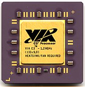
The VIA Cyrix III, later renamed the VIA C3, also used Socket 370.

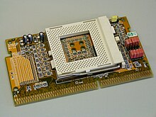
Slotkets are available that allows Socket 370 CPUs to be used on Slot 1 based motherboards. These devices are equipped with their own voltage regulator modules, in order to supply the new CPU with a lower core voltage, which the motherboard would not otherwise allow.
Socket 370 Intel processors mechanical load limits
The weight of a Socket 370 CPU cooler should not exceed 180 grams (6.3 ounces). Heavier coolers may result in damage to the die when the system is improperly handled.
Most Intel Socket 370 processors (Pentium III and Celeron) had mechanical maximum load limits which were designed not be exceeded during heat sink assembly, shipping conditions, or standard use. They came with a warning that load above those limits would crack the processor die and make it unusable. The limits are included in the table below.
| Location | Dynamic | Static |
|---|---|---|
| Die Surface | 890 N (200 lbf) | 222 N (50 lbf) |
| Die Edge | 667 N (100 lbf) | 53 N (12 lbf) |
Socket 370 Intel processors with integrated heat sink mechanical load limits
All Intel Socket 370 processors with integrated heat sink (Pentium III and Celeron 1.13–1.4 GHz) had mechanical maximum load limits which were designed not be exceeded during heat sink assembly, shipping conditions, or standard use. They came with a warning that load above those limits would crack the processor die and make it unusable. The limits are included in the table below.
| Location of integrated heat sink | Dynamic | Static |
|---|---|---|
| surface | 890 N (200 lbf) | 667 N (100 lbf) |
| edge | 556 N (125 lbf) | N/A |
| corner | 334 N (75 lbf) | N/A |
See also
References
- ^ "CPU Sockets Chart". users.erols.com. Retrieved 2009-04-16.
- ^ "Intel Pentium III Specifications" (PDF).
